cpu etiketine sahip kayıtlar gösteriliyor. Tüm kayıtları göster

5 Eylül 2010 Pazar

Bulldozer Core (AMD)


Bulldozer is the codename AMD has given to one of the next-generation CPU cores after the K10 microarchitecture for the company's M-SPACE design methodology, with the core specifically aimed at 10 watt to 100 watt TDP computing products. Bulldozer is a completely new design developed from the ground up. AMD claims dramatic performance-per-watt improvements in HPC applications with Bulldozer cores. Products implementing the Bulldozer core are planned for release in 2011.

According to AMD, Bulldozer-based CPUs will be based on advanced 32nm SOI process technology and utilize a new approach to multithreaded computer performance that, according to press notes, "balances dedicated and shared compute resources to provide a highly compact, high core count design that is easily replicated on a chip for performance scaling." In other words, by eliminating some of the redundancies that naturally creep into multicore designs, AMD hopes to take better advantage of its hardware capabilities, while utilizing less power.

The Bulldozer cores will support most of the instruction sets currently implemented in Intel processors (including SSE4.1, SSE4.2, AES, CLMUL), future Instruction sets announced by Intel (AVX), as well as future instruction sets proposed by AMD (XOP and FMA4).

As of November 2009, Bulldozer-based implementations built on 32nm SOI with HKMG are scheduled to arrive in 2011 for both servers and desktops, as the 16-core Opteron processor codenamed Interlagos and as the 4- or 8-core desktop processor codenamed Zambezi.

Bulldozer is the next-generation micro-architecture and processor design developed from the ground up by AMD. Bulldozer will be the first major redesign of AMD’s processor architecture since 2003, when the firm launched its Athlon 64/Opteron (K8) processors. Bulldozer will feature two 128-bit FMA-capable FPUs which can be combined into one 256-bit FPU. This design is accompanied with two integer cores each with 4 pipelines (the fetch/decode stage is shared). Bulldozer will also introduce shared L2 cache in the new architecture. AMD calls this design a "Bulldozer module". A 16-core processor design would feature eight of these modules, but the operating system will see each module as two physical cores.

The module is similar to an SMT core, but enhanced with a dedicated integer core and scheduler for each thread. Because the shared floating point core is significantly enhanced, performance could get beyond that of two equivalent Bobcat cores while one of the running threads is integer-only.

Bulldozer Design Breakdown

* Two tightly coupled, "conventional" x86 out-of-order processing engines which AMD internally named module
(Single-Module ==> Dual-Core, Dual-Module ==> Quad-Core, Quad-Module ==> Octa-Core etc...)
* Between 8MB to 16MB of L3 cache shared among all Modules on the same silicon die
* DDR3-1866 and Higher Memory Level Parallelism
* Dual channel DDR3 integrated memory controler (support for PC3-12800 (DDR3-1600))
* Cluster Multi-threading (CMT) Technology
* Bulldozer module consists of the following:
o 128kB L2 cache inside each module (shared between module cores)
o 4kB L1 data cache per core and 2-way 16kB L1 instruction cache per module L1 cache, Fruehe for THW
o Two dedicated integer cores
- each consist of 2 ALU and 2 AGU which are capable for total of 4 independent arithmetic or memory operations per clock per core
- duplicating integer schedulers and execution pipelines offers dedicated hardware to each of two threads which significantly increase performance in multithreaded integer applications
- second integer core increases Bulldozer module die by around 12%, which at chip level adds about 5% of total die space[9]
o Two symmetrical 128-bit FMAC (fused multiply-add (FMA) capability) Floating Point Pipelines per module that can be unified into one large 256-bit wide unit if one of integer cores dispatch AVX instruction and two symmetrical x87/MMX/3DNow! capable FPPs for backward compatibility with SSE2 non-optimized software
* 32nm SOI process with implemented first generation GF's High-K Metal Gate (HKMG)
* Support for AMD's only SSE5 128-bit instructions
- incl. three smaller supplemental extensions CVT16, XOP and FMA4 instruction set, which are now part of SSE5 specification (since May 2009 revision)
* Support for Intel's Advanced Vector Extensions (AVX) (Supports 256-Bit FP Operations via AVX)SSE4.1, SSE4.2, AES, CLMUL), future Instruction sets announced by Intel (AVX), as well as future instruction sets proposed by AMD (XOP and FMA4
* Hyper Transport Technology rev.3.1 (3.20 GHz, 6.4 GT/s, 51.6 GB/s, 16-bit uplink/16-bit downlink) [first implemented into HY-D1 revision "Magny-Cours" on the socket G34 Opteron platform in March 2010 and "Lisbon" on the socket C32 Opteron platform in June 2010]
* Socket AM3+ (AM3r2)
- 938pin(?), DDR3 support
- will retain only backwards compatiblity with previous Socket AM3/AM2 processors ("new AM3+ socket for consumer versions of Bulldozer CPUs. AM2 and AM3 processors will work in the AM3+ socket, but Bulldozer chips will not work in non-AM3+ motherboards")
* Min-Max Power Usage - 10-100 watts
* Bulldozer Module sharing levels Bulldozer module

4 Ekim 2008 Cumartesi

Intel Itanium


Itanium is the brand name for 64-bit Intel microprocessors that implement the Intel Itanium architecture (formerly called IA-64). Intel has released two processor families using the brand: the original Itanium and the Itanium 2. Starting November 1, 2007, new members of the second family are again called Itanium. The processors are marketed for use in enterprise servers and high-performance computing systems. The architecture originated at Hewlett-Packard (HP) and was later developed by HP and Intel together.


Itanium's architecture differs dramatically from the x86 architectures (and the x86-64 extensions) used in other Intel processors. The architecture is based on explicit instruction-level parallelism, with the compiler making the decisions about which instructions to execute in parallel. This approach allows the processor to execute up to six instructions per clock cycle. By contrast with other superscalar architectures, Itanium does not have elaborate hardware to keep track of instruction dependencies during parallel execution - the compiler must keep track of these at build time instead.

After a protracted development process, the first Itanium was released in 2001, and more powerful Itanium processors have been released periodically. HP produces most Itanium-based systems, but several other manufacturers have also developed systems based on Itanium. As of 2007, Itanium is the fourth-most deployed microprocessor architecture for enterprise-class systems, behind x86-64, IBM POWER, and SPARC. Intel released its newest Itanium, codenamed Montvale, in November 2007.

Intel has extensively documented the Itanium instruction set and microarchitecture, and the technical press has provided overviews. The architecture has been renamed several times during its history. HP called it PA-WideWord. Intel later called it IA-64, then Itanium Processor Architecture (IPA), before settling on Intel Itanium Architecture, but it is still widely referred to as IA-64. It is a 64-bit register-rich explicitly-parallel architecture. The base data word is 64 bits, byte-addressable. The logical address space is 2^64 bytes. The architecture implements predication, speculation, and branch prediction. It uses a hardware register renaming mechanism rather than simple register windowing for parameter passing. The same mechanism is also used to permit parallel execution of loops. Speculation, prediction, predication, and renaming are under control of the compiler: each instruction word includes extra bits for this. This approach is the distinguishing characteristic of the architecture.

The architecture implements 128 integer registers, 128 floating point registers, 64 one-bit predicates, and eight branch registers. The floating point registers are 82 bits long to preserve precision for intermediate results.

2 Şubat 2008 Cumartesi

i386


Intel Museum

i386 at CPU-Info

The Intel386 is a microprocessor which has been used as the central processing unit (CPU) of many personal computers since 1986. During its design phase the processor was code-named simply "P3", the third-generation processor in the x86 line, but is normally referred to as either i386 or just 386. The 80386 operated at about 5 million instructions per second (MIPS) to 11.4 MIPS for the 33 MHz model. It was the first x86 processor to have a 32-bit architecture, with a basic programming model that has remained virtually unchanged for over twenty years and remains completely backward compatible. Successively newer implementations of this same architecture have become literally several hundred times faster than the original i386 chip during these years.

Designed and manufactured by Intel, the i386 processor was taped-out in October of 1985. Intel decided against producing the chip before that date, as the cost of production would have been uneconomical. Full-function chips were first delivered to customers in 1986. Motherboards for 386-based computer systems were highly elaborate and expensive to produce, but were rationalized upon the 386's mainstream adoption. The first personal computer to make use of the 386 was designed and manufactured by Compaq, and Andy Grove, Intel's CEO at the time, made the decision to single-source the processor, a decision that was ultimately crucial to both the processor's and Intel's success in the market.

The range of processors compatible with the 80386 is often collectively termed x86 or the i386 architecture; today, Intel prefers the name IA-32 however.

In May 2006 Intel announced that production of the 386 would cease at the end of September 2007. Although it had long been obsolete as a personal computer CPU, Intel, and others, had continued to manufacture the chip for embedded systems, including aerospace.

23 Aralık 2007 Pazar

Intel 80286


Intel 80286 cpu-info.com

The Intel's 286, introduced on February 1, 1982, (originally named 80286, and also called iAPX 286 in the programmer's manual) was an x86 16-bit microprocessor with 134,000 transistors.

It was widely used in IBM PC compatible computers during the mid 1980s to early 1990s.

After the 6 and 8 MHz initial releases, it was subsequently scaled up to 12.5 MHz. (AMD and Harris later pushed the architecture to speeds as high as 20 MHz and 25 MHz, respectively.) On average, the 80286 had a speed of about 0.21 instructions per clock. [2] The 6 MHz model operated at 0.9 MIPS, the 10 MHz model at 1.5 MIPS, and the 12 MHz model at 2.66 MIPs.

The 80286's performance was more than twice that of its predecessors (the Intel 8086 and Intel 8088) per clock cycle. In fact, the performance increase per clock cycle may be the largest among the generations of x86 processors. Calculation of the more complex addressing modes (such as base+index) had less clock penalty because it was performed by a special circuit in the 286; the 8086, its predecessor, had to perform effective address calculation in the general ALU, taking many cycles. Also, complex mathematical operations (such as MUL/DIV) took fewer clock cycles compared to the 8086.


Having a 24-bit address bus, The 286 was able to address up to 16 MB of RAM, in contrast to 1 MB that the 8086 could directly work with. While DOS could utilize this additional RAM (extended memory) via BIOS call (INT 15h, AH=87h), or as RAM disk, or emulation of expanded memory, cost and initial rarity of software utilizing extended memory meant that 286 computers were rarely equipped with more than a megabyte of RAM.

The 286 was designed to run multitasking applications, including communications (such as automated PBXs), real-time process control, and multi-user systems.

Designer: Intel
Manufacturers: Intel, AMD, Harris, SAB
Introduction date: February 1982
Introduction speed: 6 MHz
Maximum speed: 25 MHz
Cache: -
Transistor count: 134,000
Manufacturing process: 1.5 micron

Motorola 68000


Pre-release XC68000 chip manufactured in 1979.

The Motorola 68000 is a 16/32-bit CISC microprocessor core designed and marketed by Freescale Semiconductor (formerly Motorola Semiconductor Products Sector). Introduced in 1979 as the first member of the successful 32-bit m68k family of microprocessors, it is generally software forward compatible with the rest of the line despite belonging to the 16-bit hardware technology generation. After twenty-seven years in production, the 68000 architecture remains a popular choice for new designs.


The 68000 grew out of the MACSS (Motorola Advanced Computer System on Silicon) project, begun in 1976 to develop an entirely new architecture without backward compatibility. It would be a higher-power sibling complementing the existing 8-bit 6800 line rather than a compatible successor. In the end, the 68000 did retain a bus protocol compatibility mode for existing 6800 peripheral devices, and a version with an 8-bit data bus was produced. However, the designers mainly focused on the future, or forward compatibility, which gave the M68K platform a head start against later 32-bit instruction set architectures. For instance, the CPU registers are 32 bits wide, though few self-contained structures in the processor itself operate on 32 bits at a time. The 68000 may be considered a 16-bit microprocessor which is microcoded to accelerate 32-bit tasks. The MACSS team drew heavily on the influence of minicomputer processor design, such as the PDP-11 and VAX systems, which were similarly microcoded.

In the mid 1970s, the 8-bit processor manufacturers raced to introduce the 16-bit generation. National Semiconductor had been first with its IMP-16 and PACE processors in 1973-1975, but these had issues with speed. The Intel 8086 in 1977 quickly gained popularity. The decision to leapfrog the competition and introduce a hybrid 16/32-bit design was necessary, and Motorola turned it into a coherent mission. Arriving late to the 16-bit arena afforded the new processor more integration (roughly 70000 transistors against the 29000 in the 8086), higher performance per clock, and acclaimed general ease of use.

The original MC68000 was fabricated using an HMOS process with a 3.5-micron feature size. Initial engineering samples were released in late 1979. Production chips were available in 1980, with initial speed grades of 4, 6, and 8 MHz. 10 MHz chips became available during 1981, and 12.5 MHz chips during 1982. The 16.67 MHz "12F" version of the MC68000, the fastest version of the original HMOS chip, was not produced until the late 1980s.

The 68000 had many high-end design wins early on. It became the dominant CPU for Unix based workstations, found its way into heralded computers such as the Amiga, Atari ST, Apple Lisa and Macintosh, and was used in the first generation of desktop laser printers. In 1982, the 68000 received an update to its ISA allowing it to support virtual memory by conforming to the Popek and Goldberg virtualization requirements. The updated chip was called the 68010. A further extended version which exposed 31 bits of the address bus was also produced, in small quantities, as the 68012.

To support lower-cost systems and control applications with smaller memory sizes, Motorola introduced the 8-bit compatible MC68008, also in 1982. This was a 68000 with an 8-bit data bus and a smaller (20 bit) address bus. After 1982, Motorola devoted more attention to the 68020 and 88000 projects.

3 Kasım 2007 Cumartesi

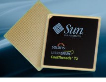
UltraSPARC T2


Sun UltraSPARC T2

spec.org Q4 2007 Benchmarks


* Up to 8 cores, up to 64 threads per processor
* Dual 10Gbit Ethernet and PCI-E integrated onto chip
* Logical Domains (LDoms) for hardware virtualization with up to 64 OS instances
* Cryptographic processing at wire speeds


Single-chip SPEC CPU scores, based on tests that delivered 78.3 est. SPECint_rate2006 and 62.3 est. SPECfp_rate2006.

The UltraSPARC T2 is the first major processor whose blueprints are available under a free software license, namely the GPL.

3 Eylül 2007 Pazartesi

Cell


Cell Wikipedia

Cell Broadband Engine resource center

Cell Broadband Engine (SONY)

Cell is a microprocessor architecture jointly developed by a Sony, Toshiba, and IBM, an alliance known as "STI." The architectural design and first implementation were carried out at the STI Design Center over a four-year period beginning March 2001 on a budget reported by IBM as approaching US$400 million. Cell is shorthand for Cell Broadband Engine Architecture, commonly abbreviated CBEA in full or Cell BE in part. Cell combines a general-purpose Power Architecture core of modest performance with streamlined coprocessing elements which greatly accelerate multimedia and vector processing applications, as well as many other forms of dedicated computation.

The first major commercial application of Cell was in Sony's PlayStation 3 game console. Mercury Computer Systems has a dual Cell server, a dual Cell blade configuration, a rugged computer, and a PCI Express accelerator board available in different stages of production. Toshiba has announced plans to incorporate Cell in high definition television sets. Exotic features such as the XDR memory subsystem and coherent Element Interconnect Bus (EIB) interconnect appear to position Cell for future applications in the supercomputing space to exploit the Cell processor's prowess in floating point kernels. IBM has announced plans to incorporate Cell processors as add-on cards into IBM System z9 mainframes, to enable them to be used as servers for MMORPGs.

The Cell architecture includes a novel memory coherence architecture for which IBM received many patents. The architecture emphasizes efficiency/watt, prioritizes bandwidth over latency, and favors peak computational throughput over simplicity of program code. For these reasons, Cell is widely regarded as a challenging environment for software development. IBM provides a comprehensive Linux-based Cell development platform to assist developers in confronting these challenges. Software adoption remains a key issue in whether Cell ultimately delivers on its performance potential. Despite those challenges, research has indicated that Cell excels at several types of scientific computation.

In November 2006, David A. Bader at Georgia Tech was selected by Sony, Toshiba, and IBM from more than a dozen universities to direct the first STI Center of Competence for the Cell Processor. This partnership is designed to build a community of programmers and broaden industry support for the Cell processor.

In 2000, Sony Computer Entertainment, Toshiba Corporation, and IBM formed an alliance ("STI") to design and manufacture the processor.

The STI Design Center in Austin, Texas opened in March 2001. The Cell was designed over a period of four years, using enhanced versions of the design tools for the POWER4 processor. Over 400 engineers from the three companies worked together in Austin, with critical support from eleven of IBM's design centers.

During this period, IBM filed many patents pertaining to the Cell architecture, manufacturing process, and software environment. An early patent version of the Broadband Engine was shown to be a chip package comprising four "Processing Elements," which was the patent's description for what is now known as the "Power Processing Element." Each Processing Element contained 8 "APUs," which are now referred to as SPEs on the current Broadband Engine chip. Said chip package was widely regarded to run at a clock speed of 4 GHz and with 32 APUs providing 32 GFLOPS each, the Broadband Engine was shown to have 1 teraflops of raw computing power.

In March 2007 IBM announced that the 65 nm version of Cell BE is in production at its plant in East Fishkill, New York.